PCB or printed circuit board which means a printed circuit board, is a thin board made of a kind of fiber as its insulating medium, which is used to lay electronics components, in pairs and in concatenation, where one side is coated copper to soldering legs component. PCB or Printed Circuit Board also has conductor lines made of copper and serves to connect between one component with other components. You should know about PCB Assembly.
The copper thickness on PCB or Printed Circuit Board of various kinds, there are 35 micrometers, there are also 17-18 micrometers. Other materials are phenolic or Pertinax paper, usually brown, this type of material is more popular because of its cheaper price. There are also made from fiberglass materials that are used for Through hole plating, because the material is stronger and not easily bent in comparison with Pertinax.
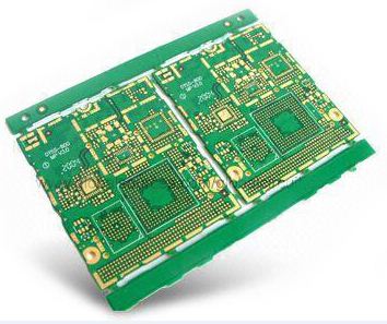
PCB or Printed Circuit Board has several kinds in accordance with its function, in example one side (commonly used in electronic circuits such as radio, TV, etc.), two sides (can be used to connect components on both sides) and multi-side in use as a conductor medium, for example in PC circuits).
In the making, many ways that can be done, either manually or conventionally to use the software as a tool help, namely:
- Photoresist technique, in this process, required some tools and materials, namely: UV Lamp, Positive Solution-20, and NaOH solution.
- Screen printing Technique, this technique is almost the same as regular screen printing where required materials such as screen-screen, screen printing, paint, and others.
- Direct Print, in this process, used a special technique to copy the layout that is used a special printer machine that has been modified.
- Transfer Paper technique, this technique is my cheapest and easy way.
In addition to the four ways above, there is also a way of making by using software, where first the electronic designer will create or design it first in the computer. Therefore, PCB Assembly cost is various. This can simplify or reduce the error rate because when the error is found, the designer will edit and correct the design before printing.
We can get a lot of software on the internet to be able to help us make its layout automatically based on the scheme we make. You also can try the Aluminum PCB.